Kristr is now Maketronics | Visit www.make-tronics.com for new updates

The best Accessories for your Raspberry Pi

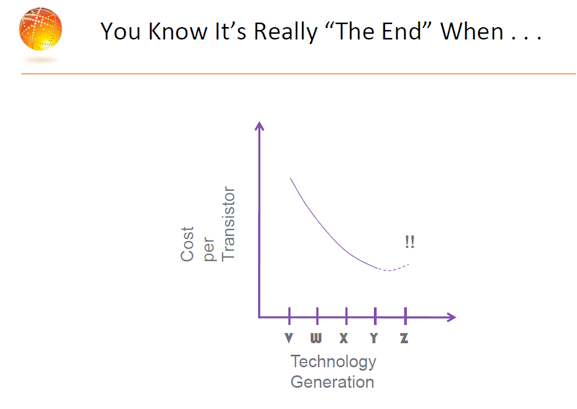
In 2017, The MagPi Magazine – the authority Raspberry Pi magazine – reported that over 12.5 million of the Raspberry Pi single-board PCs (SBCs) had been sold since the 2012 presentation of the primary form. The Pi has not just shown to be a #1 of specialists, producers and designers the same, it has even gotten the interest of AI scientists at Microsoft.

Combined with its blast in fame is the rundown of frill that supplement this SBC. Coming up next is a rundown of suggested extras for you, the Raspberry Pi fan.

If, notwithstanding, you’re not there yet, we can assist you with the beginning. So we should begin with a pack.

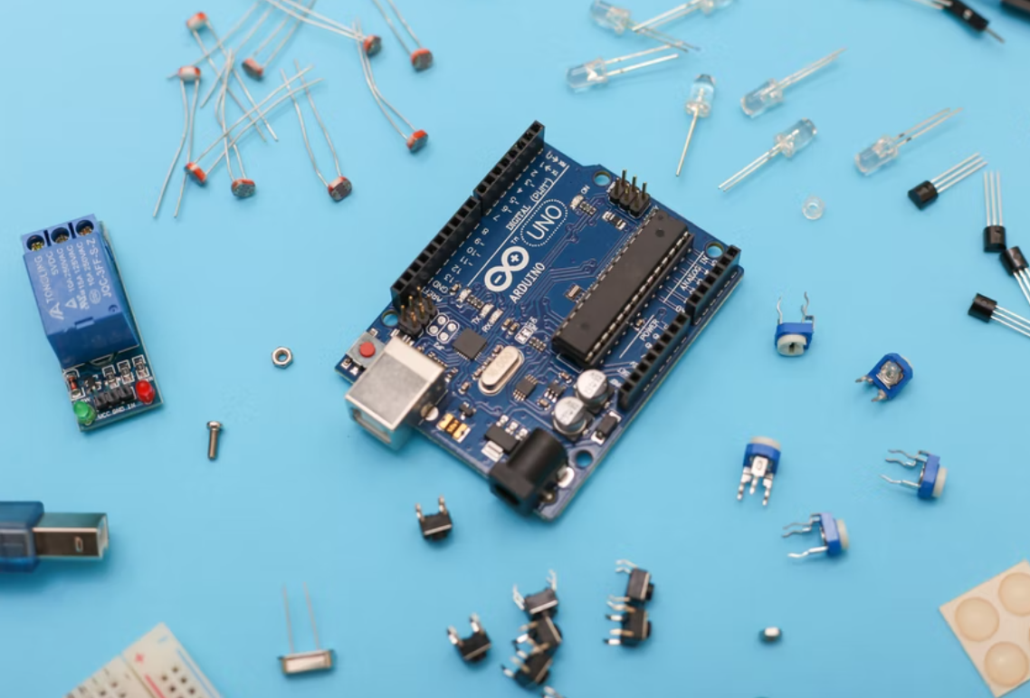
The starter pack for the new Raspberry Pi proprietor

We suggest Raspberry Pi Foundation’s own starter pack for an overall investigation of the SBC. The unit incorporates a Raspberry Pi 3 Model B, 8-GB or 16-GB NOOBS SD card, case, a 2.5-A multi-locale power supply, 1-m HDMI link, optical mouse, and a console with top-notch scissor-switch activity.

What we truly like about this pack is that it accompanies a duplicate of “Undertakings in Raspberry Pi.” The writer, Carrie Anne Philbin, guides you through your new SBC obtaining, exhibits how to compose programs in Scratch and Python, utilizes engineer devices like Minecraft Pi and Sonic Pi and examines a few first ventures.

Equipped with a Raspberry Pi, now is the ideal time to take a gander at ways you can get the majority of your SBC – through embellishments and direction.

Raspberry Pi Cookbook

First up is the book by Simon Monk that goes past the manual in the starter pack to give you north of 200 recipes or tasks. It will show you how to set up and deal with the board, associate it to an organization, work with its Linux OS, program in Python, control other equipment including engines, secure data from sensors and much more. The Raspberry Pi Cookbook is simply $39.99.

To dive further into the Python programming language, we additionally suggest Python for Microcontrollers: Getting Started with MicroPython. This book won’t just show you the Pi’s Python local language yet arm you with eight extra model tasks.

Google AIY Voice Kit for Raspberry Pi

To rapidly construct an all set venture – in about 90 minutes level – attempt AIY Projects’ Google AIY Voice Kit. For just $29.99, you can construct yourself your own voice-actuated home right hand.

The pack incorporates a voice Hardware-Attached-on-Top (HAT) embellishment board, voice HAT mouthpiece board, 3-in. speaker, arcade-style pushbutton, edge and plastic stalemates. You’ll should simply supply a Raspberry Pi 3 board, a SD card, size “00” Phillips screwdriver and some Scotch tape.

Happiness Bonnet

In the event that you are wanting to construct a gaming framework, you’ll require a game regulator. Adafruit’s Joy Bonnet sits on top of a Pi Zero to empower arcade-like control. For just $15.61, this deal regulator is a completely collected HAT, and that implies you don’t have to bind anything. All you want to do is to introduce your content on the Pi and transfer your emulator, like the RetroPie or the EmulationStation.

You can likewise utilize the Joy Bonnet with Pi A+ or B+/2/3, however it’s the Pi Zero that it fits the best.

Raspberry Pi Sense HAT

Prepared to utilize sensors to assemble games, control other equipment or lead science tests? The Raspberry Pi Sense HAT appends a few on-board sensors on top of the Raspberry Pi by means of the GPIO pins. It was made for the Astro Pi mission and was sent off to the International Space Station in December 2015 to perform science tests.

This HAT incorporates a gyro, accelerometer, magnetometer, temperature sensor, barometric tension sensor and a mugginess sensor. A 8 × 8 RGB LED grid will show information from the sensors, and you can utilize a five-button joystick to connect with your task here on Earth.

You can purchase the Sense HAT for $70.39 and download Raspberry Pi Foundation’s Python library here to control it.

Adafruit 7-in. LCD TFT touchscreen

Transform the Pi into a tablet with Adafruit’s 7-in. touchscreen, which gives you a 1,024 x 600 goal that is a decent counterpart for inserted processing needs.

You can drive it over USB and contribution over HDMI. Included is a resistive touchscreen-to-mouse regulator (AR1100) – a board that handles A/D change – as well as adjustment programming. A wired PCB with buttons permits you to enter the showcase’s menu for changing splendor, differentiation and variety.

On the off chance that you are fostering a LED divider show, consider adding an Adafruit RGB Matrix HAT to make a looking over show utilizing 16 x 32, 32 x 32, and 32 x 64 RGB LED frameworks with HUB75 associations.

The Pi-Top Laptop
For the people who are considering utilizing the Pi a dainty client or more, the Pi-Top will get you an open-source PC for just $299.99. You’ll get a 14-in. 1080p LCD, complete with a nook that incorporates a console, trackpad and battery, a PCB to deal with the associations between the Pi and the remainder of the framework, 8-GB SD card, links and charger.

What’s best about this Pi-to-Laptop converter is that gathering is pretty much as simple as “clicking” the provided parts into place.

Pimoroni SkyWriter HAT

Our last pick is an extra that will acquaint you with the developing signal control market. With the SkyWriter HAT, you can carry the ability to utilize signals to your Raspberry Pi (Models 3, 2, A+, B+ and Zero) for just $18.99.

The HAT has an electrical close field 3D/motion sensor that can recognize your developments to the extent that 5 cm away and can work from behind a non-conductive material-like texture. It tracks finger developments and signals like tap/twofold tap and finger flicks.

To get more familiar with these frills and investigate extra choices, go to Arrow.com. On the off chance that you pick to make a buy and spend more than $20, you’ll appreciate free one-day transport.

Less expensive Way To Make Flexible Semiconductors?

MIT engineers have fostered a strategy to manufacture adaptable ultrathin semiconducting movies produced using GaAs, GaN, and lithium fluoride – materials that show preferable execution over silicon yet as of not long ago have been restrictively costly to create in utilitarian gadgets.
The new strategy, scientists say, gives a financially savvy technique to create adaptable hardware produced using any blend of semiconducting components, that could perform better compared to current silicon-based gadgets.

“We’ve opened up a method for making adaptable gadgets with such countless different material frameworks, other than silicon,” says Jeehwan Kim, the Class of 1947 Career Development Associate Professor in the divisions of Mechanical Engineering and Materials Science and Engineering. Kim imagines the method can be utilized to produce minimal expense, elite execution gadgets like adaptable sun-powered cells, and wearable PCs and sensors.

Subtleties of the new method are accounted for in Nature Materials. Notwithstanding Kim, the paper’s MIT co-creators incorporate Wei Kong, Huashan Li, Kuan Qiao, Yunjo Kim, Kyusang Lee, Doyoon Lee, Tom Osadchy, Richard Molnar, Yang Yu, Sang-hoon Bae, Yang Shao-Horn, and Jeffrey Grossman, alongside scientists from Sun Yat-Sen University, the University of Virginia, the University of Texas at Dallas, the US Naval Research Laboratory, Ohio State University, and Georgia Tech.

In 2017, Kim and his partners concocted a strategy to create ‘duplicates’ of costly semiconducting materials utilizing graphene. They found that when they stacked graphene on top of an unadulterated, costly wafer of semiconducting material, for example, GaAs, then streamed molecules of gallium and arsenide over the stack, the particles seemed to connect here and there with the fundamental nuclear layer, as though the halfway graphene were undetectable or straightforward. Subsequently, the iotas gathered into the exact, single-translucent example of the basic semiconducting wafer, framing a precise duplicate that could then effectively be stripped away from the graphene layer.

The procedure, which they call ‘far off epitaxy’ gave a reasonable method for creating different movies of GaAs, utilizing only one costly fundamental wafer.

Not long after they announced their most memorable outcomes, the group puzzled over whether their procedure could be utilized to duplicate other semiconducting materials. They had a go at applying distant epitaxy to silicon, and furthermore, germanium yet found that when they streamed these molecules over graphene they neglected to collaborate with their individual basic layers. It was as though graphene, beforehand straightforward, turned out to be out of nowhere obscure, keeping iotas of silicon and germanium from “seeing” the molecules on the opposite side.

As it works out, silicon and germanium are two components that exist inside a similar gatherings of the intermittent table of components. In particular, the two components have a place in bunch four, a class of materials that are ionically unbiased, meaning they have no extremity.

“This gave us a clue,” says Kim.

Maybe, the group contemplated, molecules can interface with one another through graphene assuming that they have some ionic charge. For example, on account of GaAs, gallium has a negative charge at the connection point, contrasted and arsenic’s positive charge. This charge distinction, or extremity, may have assisted the iotas with interfacing through graphene as though it were straightforward, and to duplicate the basic nuclear example.

“We tracked down that the communication through not entirely set in stone by the extremity of the particles. For the most grounded ionically reinforced materials, they cooperate even through three layers of graphene,” Kim says. “It’s like the manner in which two magnets can draw in, even though a dainty piece of paper.”

Opposites are inclined toward one another

The specialists tried their speculation by utilizing far-off epitaxy to duplicate semiconducting materials with different levels of extremity, from unbiased silicon and germanium to somewhat spellbound GaAs, and lastly, exceptionally captivated lithium fluoride – a superior, more costly semiconductor than silicon.

They tracked down that the more prominent the level of extremity, the more grounded the nuclear communication, even, now and again, through numerous sheets of graphene. Each film they had the option to deliver was adaptable and simply tens to many nanometers thick.

The material through which the molecules connect additionally matters, the group found. Notwithstanding graphene, they explored different avenues regarding a halfway layer of hexagonal boron nitride (hBN), a material that looks like graphene’s nuclear example and has a comparative Teflon-like quality, empowering overlying materials to effortlessly strip off whenever they are replicated.

Nonetheless, hBN is made of oppositely charged boron and nitrogen iotas, which create an extremity inside the actual material. In their tests, the scientists found that any iotas streaming over hBN, regardless of whether they were exceptionally energized themselves, couldn’t connect with their fundamental wafers totally, proposing that the extremity of both the molecules of interest and the transitional material decides if the particles will cooperate and frame a duplicate of the first semiconducting wafer.

“Presently we truly comprehend there are rules of nuclear cooperation through graphene,” Kim says.

With this new getting it, he says, specialists can now essentially check out at the intermittent table and pick two components of the inverse charge. When they secure or create a fundamental wafer produced using similar components, they can then apply the group’s far-off epitaxy procedures to manufacture various, precise duplicates of the first wafer.

“Individuals have for the most part utilized silicon wafers since they’re modest,” Kim says.

“Presently our strategy opens up a method for utilizing higher-performing, nonsilicon materials. You can simply buy one costly wafer and duplicate it again and again, and continue to reuse the wafer. Also, presently the material library for this procedure is completely extended.”

Kim imagines that far-off epitaxy can now be utilized to create ultrathin, adaptable movies from a wide assortment of beforehand outlandish, semiconducting materials – as long as the materials are produced using iotas with a level of extremity. Such ultrathin movies might actually be stacked, one on top of the other, to deliver little, adaptable, multifunctional gadgets, like wearable sensors, adaptable sunlight-based cells, and even, in the far off future, “cellphones that connect to your skin.”

“In brilliant urban areas, where we should put little PCs all over the place, we would require low power, profoundly touchy registering and detecting gadgets, produced using better materials,” Kim says. “This [study] opens the pathway to those gadgets.”

UMC Breaks into 14nm

TAIPEI — United Microelectronics Corp. (UMC), Taiwan’s second-largest foundry, has started its first production of 14nm products, narrowing a technology gap with its larger competitors such as Taiwan Semiconductor Manufacturing Co. (TSMC) and Samsung.

UMC said that, during the second quarter this year, 14nm accounted for 1 percent of its total revenue for the first time.

In the meantime, the company slashed its 2017 capital expenditure budget to $1.7 billion from the $2 billion it had earmarked earlier this year. UMC’s CAPEX for 2016 was $2.8 billion.

“Operational efficiency will be the focus,” said Jason Wang, the newly appointed co-president of UMC, at an event to announce the company’s second-quarter results. “We are aligning to the current demand outlook.”

The company said it may cede competition at the 10nm and 7nm nodes to larger rivals TSMC and Samsung, where UMC said there will be “less demand”. UMC said it will focus on addressable markets where there is still plenty of room to grow.

While the company declined to forecast its 2018 CAPEX, UMC said it will be “cautious” with capital expenditure plans in the future.

No. 1 foundry TSMC plans to hold steady, with capital expenditures reaching about $10 billion this year. In 2016, the company’s CAPEX came in at $10.4 billion. TSMC, Samsung, and Intel are the top three spenders in the chip industry.

UMC’s pared Capex plan comes at the same time as Samsung reportedly aims to grab a bigger slice of the foundry business. Samsung plans to triple its foundry share as it aims for the No. 2 position after TSMC.

Mainstay Products Solid

Demand for UMC’s mainstay 28nm and 40nm products held firm during the second quarter. UMC’s 28nm brought in 17 percent of the company’s overall revenue during the second quarter, the same percentage as in the first quarter this year. UMC’s 40nm accounted for a 28 percent chunk of overall revenue in the second quarter, dipping from 29 percent in the first quarter.

Due to a weaker outlook for 28nm, the company forecast that its 28nm high-k metal gate (HKMG) business may decline during the next few quarters this year.

Analysts at the event noted that UMC may face increasing competition from Chinese foundries such as Semiconductor Manufacturing International Corp. (SMIC) which are ramping up 28nm poly gate and SiON gate dielectric (poly-SiON) production.

UMC said that while demand for 28nm HKMG is “lagging expectations,” the company expects full loading for 28nm poly-SiON in the foreseeable future.

UMC makes most of its 28nm products at its Tainan fab in southern Taiwan and is ramping up production at its new fab in Xiamen, China, that’s a joint venture with the local government. By the end of this year, the company expects to have 39,500 12-inch wafers per month — including about 5,000 wafers at the Xiamen fab — in 28nm process technology.

While TSMC and Samsung are starting up production of 10nm, UMC has targeted 14nm as its most advanced technology node. In the meantime, TSMC has been filling gaps in its legacy 28nm process to blunt the competition.

TSMC has increased capacity for 28nm, which accounted for more than a quarter of its revenue during the second quarter of this year. The company, which has counted on 28nm as a cash cow for more than five years, is hanging on to a 90 percent share of the market even as rivals such as UMC, Intel, and SMIC are trying to grab a chunk of that business.

UMC said its capacity utilization during the second quarter was 96 percent, unchanged from the first quarter. The company said it expects the utilization rate to fall to the low 90 percent range during the third quarter this year.

Earlier this year, UMC’s board of directors appointed Jason Wang and SC Chien as co-presidents of the company. Chien will be in charge of fab operations and technology development while Wang will be responsible for business management and corporate strategy.

11 Views of Vintage Microcomputers

MOUNTAIN VIEW, Calif. — Fans of systems from the beginning of the personal computer era in the 1970s and 80s gathered last weekend at the Vintage Computer Festival West. The event hosted by the Computer History Museum here showcased some minicomputers and workstations in addition to early microcomputers.

A panel session with a number of the early Commodore engineers talked about their once-popular, early home PCs. Commodore International started as a calculator company. Later it bought MOS Technologies, the manufacturer of the iconic 6502 microprocessor used in the Apple II, and entered the home computer market. A no-show for the panel was Chuck Peddle, considered the father of the 6502 and the man who convinced Commodore CEO Jack Tramiel to move beyond calculators and into computers.

Two panels discussed the Xerox PARC Alto workstation, the inspiration for modern personal computers from both Apple and Microsoft. The Alto was made in the mid-1970s, yet almost all the bipolar TTL chips inside systems at the event were still working. Engineers only had to replace one inverter chip.

Engineers who restored the systems said their biggest challenge was cobbling into one working machine piece from multiple salvaged Altos using different disk drives, disk controllers, and other mismatched peripherals.

Clubs and private collectors showed their vintage computers and related peripherals at the event, with one booth specializing in every flavor of the floppy disk. Attendees could buy their own classic products at a mini flea market for computers, peripherals, chips, manuals, and other related odds and ends.

Server DRAM Supply Expected to Remain Tight

SAN FRANCISCO — Server DRAM revenue among the top three DRAM vendors — Samsung Electronics, SK Hynix, and Micron Technology — rose by 30 percent sequentially in the second quarter as the tight supply of DRAM chips continued to lift average selling prices, according to market watcher DRAMeXchange. The firm expects server DRAM supply to remain tight throughout the remainder of 2017.

Despite product mix adjustments, suppliers had trouble meeting the various growing demands of the DRAM market, said DRAMeXchange, a unit of market research firm TrendForce that tracks memory chip pricing.

“Thanks to the increase in the average memory density of server systems, as evidenced by the adoption of high-density 32GB RDIMMs and 64GB LRDIMMs in this year’s first half, the profit margin of server DRAM surged,” said Mark Liu, a DRAMeXchange analyst, in a press statement.

DRAMeXchange said it expects the penetration rate of DDR4 2666MHz modules to rise in the second half of this year due to the introduction of servers based on Intel’s Purley platform.

South Korea’s Samsung, the leading memory supplier and the leader in server DRAM market share, saw its second-quarter server DRAM revenue rise by 36.5 percent sequentially to reach nearly $2 billion, DRAMeXchange said. Samsung continues to benefit from a commanding lead in the overall DRAM market and an overall lead in manufacturing technology, according to the firm.

TI’s three high-quality audio floating-point DSP processors

Texas Instruments (TI) declared the send off of three new drifting point DSPs in light of the TMS320C67x™ DSP series, further lessening the advancement cost of excellent sound items. The new center in light of C67x™ DSP has high-productivity C language proficiency, and its VLIW engineering fundamentally further develops application execution.
The TMS320C6722, TMS320C6726 and TMS320C6727 DSPs cost up to 130 MFLOPS for each dollar, empowering sound specialists to coordinate unrivaled DSP handling execution in an assortment of sound applications, including broadcasting, gatherings, instruments and expert sound. Because of clients’ requests for higher sound execution, TI made the C672x gadget for excellent sound applications where sound quality and cost-adequacy are basic.

TI has acknowledged numerous parts of improvement and development through C672x drifting point gadgets, and to completely fulfill market need, these gadgets have code similarity with the full scope of C67x™ DSP items. C672x gadgets have the accompanying upgrades:

·Increment the quantity of inward registers from 32 to 64 to upgrade the presentation of the register-bound part and simplify compiler enhancement and more straightforward.

·Increment the quantity of equal drifting point “add directions” from 2 to 4, expanding the FFT handling execution by 20%.

·Increment the limit of the guidance store from 4K to 32K to diminish the miss punishment of the guidance reserve.

·Carry out the dMAX DMA motor to decrease the processor’s heap during the impact handling to zero in on the execution of off-chip memory access.

·Give new blended accuracy guidelines, including 32’32-piece increase directions with a 64-digit result and 32’64-piece augmentation with a 64-bit result to work on the exhibition of excellent FIR and IIR channels in high-testing rate, low-recurrence sound applications Performance productivity.

·With a level memory model, it can accomplish more steady application execution. Together, these advancements can work on the presentation of some certifiable sound applications by over 20%. For instance, MP3 unraveling as of now just involves 16MHz C672x DSP, which is lower than 20MHz of C6713 DSP, while 10-band balancer deciphering just possesses 6MHz C672x DSP, which is lower than C6713 DSP’s 17MHz. C672x gadgets have a clock recurrence of 200-300MHz, with 256KB of SRAM and 32KB of guidance store.

C672x utilizes peripherals chose explicitly for sound applications. Fringe sets differ with explicit processors, yet C672x gadgets incorporate 3 McASPs, 2 SPIs, 1 HPI, 1 RTI, 1 EMIF, 2 I2C, 1 PLL, and 1 dMAX motor. TI likewise declared the send off of the Professional Audio Development Kit (PADK) created by Lyrtech Signal Processing. With PADK, engineers can rapidly assess the exhibition of C672x gadgets and promptly start item advancement without fostering their own model circuit loads up first, consequently shortening item configuration time.

PADK impeccably coordinates C6727 DSP and TI’s pay simple innovation, including TI’s Burr-Brown product offering A/D and D/A converters. Likewise, PADK has been adapted to very good quality expert sound applications. The PADK planned by Lyrtech not just completely exhibits the proficiency of the C672x DSP, yet additionally incorporates certifiable expert sound calculations and programming models that can show the center presentation and sound handling capacities.

The on-board extension space gives adaptable I/O availability, permitting designers to assess other simple parts to accomplish different item costs. Notwithstanding PADK, TI additionally gives a DSP advancement instrument planned along with the equipment, to utilize the C language to accomplish very high unique execution. Code Composer Studio™ (TMDSCCSALL-1) contains TI’s streamlined C language compiler, which dispenses with the requirement for gathering code much of the time, making it more straightforward to keep up with the code base.

For video conferencing and different applications that need to blend video and sound, designers can save time and diminish responsibility since they can utilize similar apparatuses to foster sound and video subsystems. Notwithstanding sound applications, C672x gadgets are likewise appropriate for supporting numerous different applications that utilization drifting point innovation, including biometrics, clinical and modern applications. C67x™ drifting point DSP has been broadly utilized in the fields of advanced sound and buyer gadgets. It is the center innovation of the Aureus sound DSP series. It very well may be utilized in the A/V recipient and interactive media of organizations like Harman/Kardon, JVC, Yamaha and Denon. /Perform multi-direct sound handling in the game framework.

Likewise, TI’s Burr-Brown product offering additionally gives a wide scope of high-accuracy simple and inconsistent message IC answers for meet the superior execution signal handling needs of the expert sound market.

RoHS background,what is RoHS compliant?

Foundation

In 1998, the European Union found that alarmingly a lot of perilous waste were being unloaded into landfill destinations. Drifts additionally demonstrated that the volumes were probably going to grow 3-5 times quicker than normal city squander. This featured a gigantic, and developing, wellspring of ecological contamination.In request to resolve the issues this data raised, the part conditions of the EU chose to make the Waste Electrical and Electronics Equipment (WEEE) mandate, whose intention was to:

I. Work on makers’ plans, to lessen the formation of waste

ii. Make producers liable for specific periods of waste administration

iii. Separate assortments of electronic waste (from different sorts of waste)

iv. Make frameworks to further develop treatment, reject, and reusing of WEEE

The WEEE mandate gave the starting points of the ongoing impending regulation. Notwithstanding, beginning around 1998, a draft proposition called EEE (Environment of Electrical and Electronics Equipment) was likewise presented similarly. Presently, as the execution of this approach becomes imminent, this strategy is for the most part alluded to as the ROHS Directive.

What Is RoHS?

The ROHS mandate is frequently alluded to as “Lead-Free” regulation. This is definitely not an extremely precise moniker, since it stretches out to different contaminations also. The appropriate name for ROHS is:

Mandate 2002/95/EC

“The limitation of the utilization of specific dangerous substances in electrical and electronic gear” and it applies to the accompanying substances:

· Lead
· Mercury
· Cadmium
· Hexavalent Chromium
· PBB
· PDBE

To follow the EU ROHS regulation, these substances should either be eliminated, or should be decreased to inside greatest allowed fixations, in any items containing electrical or electronic parts that will be sold inside the European Union.
The capacitors, resistors, diodes, and semiconductors ought to be ROHS

How to choose a good adjustable capacitor?

Capacitors are essential circuit components that store and give charges on request, and are the fundamental parts of detached circuits and assistant parts of dynamic circuits. While planning a circuit, designs frequently need to weigh many variables, for example, picking a proper capacitor or a customizable capacitor. Albeit most circuits decide to utilize fixed capacitors, at times, the utilization of customizable capacitors is more great or vital. Then, I will take more time to look further into movable capacitors and assist you with settling on your optimal decision.
What Is An Adjustable Capacitor?

The tunable capacitor is a variable capacitor, which permits a little scope of variable tuning, for example, the recurrence worth of the oscillator or the quantity of rises and falls. Furthermore, assuming the worth movements during the existence of the gadget, the customizable capacitor can be recalibrated on a case by case basis. For delicate applications, for example, attractive reverberation imaging (MRI), any precariousness because of time or temperature might influence the picture yield. Picking a flexible capacitor can assist with streamlining gadget execution.

As a rule, albeit the expense of customizable capacitors is somewhat higher than that of fixed capacitors, it additionally gives more prominent adaptability. Be that as it may, when the issue of capacitance exactness is experienced, the expense of utilizing a proper capacitor with high precision will be higher, so movable capacitors might be more financially savvy. Albeit the volume of fixed capacitors was altogether more modest than that of movable capacitors, the rise of chip movable capacitors has compensated for this hole.

Not at all like fixed capacitors, which have a decent capacitance esteem, customizable capacitors can change the exhibition of dynamic and latent circuits. The worth of the customizable capacitor is for the most part between 1 pF and 2 pF, however it can likewise be extended to 200 pF or more. Fixed capacitors store charges through two fixed metal layers, however in flexible capacitors, it is important to change the distance between these metal layers or change the region of the powerful region to change the capacitance.

Fundamental Structure Of Adjustable Capacitor

Likewise with fixed capacitors, in customizable capacitors, an assortment of dielectric materials are utilized as electrical protecting materials between metal layers or other metalized surfaces. The exactness and consistency of the dielectric impact the precision and dependability of the flexible capacitor capacitance.

Flexible capacitors can be planned into cylindrical and plate-like designs. By moving the cylinder inside the external metalized dielectric tube, the capacitance will change, and as the cylinder covers with more fixed metal inward dividers, the capacitance will increment. You can likewise utilize a cylinder and a bunch of versatile concentric metal rings to accomplish this change. These rings are introduced in a bunch of fixed equal rings. As the rings are locked in, the capacitance increments. In rounded movable capacitors, a cylinder associated with a change screw can be utilized to change the capacitance.

How To Choose The Dielectric In A Tunable Capacitor?

In tunable capacitors, an assortment of dielectrics can be utilized to occupy the space between the metal layers. These materials incorporate air, pottery, glass, PTFE, and sapphire. Among them, air gives the least protection and is extremely restricted as far as voltage dealing with ability and capacitance esteem. Movable capacitors that utilization glass, quartz and polytetrafluoroethylene as dielectric materials can give adequate protection at higher evaluated voltages and can acquire higher capacitance values.

In high-recurrence applications with higher necessities for quality (Q) component and series reverberation recurrence, multi-turn movable capacitors utilizing air, sapphire or PTFE as dielectric materials can give the most reduced misfortune and the best generally speaking exhibition. How much protection given by the dielectric material influences the appraised voltage of the capacitor, which is generally communicated as far as its endure voltage (DWV). For instance, polytetrafluoroethylene has a higher dielectric consistent than air (the dielectric steady of air is equivalent to 1), which can give a higher endure voltage (DWV) for customizable capacitors-around 15,000V or higher.

Flexible capacitors utilizing fired dielectrics are little in size, economical, and can be bundled on tape and are appropriate for computerized producing machines. The capacitance scope of this sort of capacitor can be set to around 40 pF, which is entirely reasonable for applications that need to address the issues of little size and minimal expense. Notwithstanding, clay customizable capacitors are regularly restricted by temperature soundness, and the exhibition will diminish as the capacitance increments. These parts have a quality element of around 1,500 at 1 MHz and an ostensible temperature coefficient of 0 to 750 ppm/°C. The capacitance float range is about ±1% to ±5%, and the most extreme endure voltage (DWV) doesn’t surpass 220 VDC.

The movable capacitor with sapphire as the dielectric is entirely sturdy. Its dielectric steady worth doesn’t change with recurrence, has high mechanical strength and dampness obstruction, and its misfortune is exceptionally low, even over 10 GHz. The Giga-Trim flexible capacitor of Lou’s Capacitor involves sapphire as the dielectric and is a high-strength scaled down customizable capacitor with magnificent electrical qualities. This kind of capacitor can endure high-temperature welding, over-tuning and unpleasant activity. Sapphire has magnificent dielectric and protection properties, so it can endure high breakdown voltage.

What is mcu?

what is mcu?Microcontroller Unit (MCU), otherwise called a solitary chip microcomputer or a solitary chip microcomputer, decreases the recurrence and determinations of a Central Process Unit (CPU) suitably, Timer, USB, A/D change, UART, PLC, DMA and other fringe interfaces, and even LCD driver circuits are coordinated into a solitary chip to shape a chip-level PC with various mixes of controls for various applications. Like cell phones, PC peripherals, controller, to car hardware, modern stepper engine, robot arm control, can see the figure of the MCU.

As per the transport or information register width, the microcontroller is partitioned into 1, 4, 8, 16, 32 or even 64-cycle microcontroller. The vast majority of the 4-bit MCUs are utilized in number crunchers, vehicle meters, vehicle hostile to burglary gadgets, pagers, cordless telephones, CD players, LCD drive regulators, LCD game control center, youngsters’ toys, scales, chargers, , Thermometer and hygrometer, controller and simple to use cameras; 8-cycle MCU the greater part of the applications in the meter, engine regulator, electric toys, inverter climate control systems, pagers, fax machines, CallerID, guest ID , CRT screens, consoles and USB; 8-bit, 16-bit microcontrollers are primarily utilized in everyday control regions, by and large don’t utilize the working framework, 16-bit MCU most utilized in cell phones, advanced cameras and video recorders, Most 32-bit MCUs are utilized in Modem, GPS, PDA, HPC, STB, Hub, Bridge, Router, workstations, ISDN telephones, laser printers and shading fax machines; 32-digit applications for complex organization tasks, sight and sound handling, and so forth , Generally utilize the installed working framework. Most 64-cycle MCUs are utilized in very good quality workstations, sight and sound intuitive frameworks, progressed computer game players like SEGA’s Dreamcast and Nintendo’s GameBoy, and progressed terminals.

8-digit MCU working recurrence between 16 ~ 50MHz, underscoring the basic presentation, minimal expense applications, the present absolute market worth of the MCU actually has a specific status, and numerous MCU administrators have additionally kept on creating energy-saving 8bit MCU recurrence change plan to answer Green item improvement requirements of the times.

16-digit MCU, 16-cycle processing, 16/24-bit addressability and recurrence in the 24 ~ 100MHz standard details, some 16bit MCU extra 32-bit in addition to/short/duplicate/partition unique guidelines. As the 32bit MCU shows up and keeps on reducing costs and 8bit MCU is basic and tough and modest minimal expense advantage, trapped in the center 16bit MCU market keeps on being fit into the least extent of transportation items.

32-bit MCU market can be said that the standard, the single proposal in the 1.5 to 4 US dollars, a large portion of the working recurrence between 100 ~ 350MHz, the execution of better execution, application types are very assorted. Be that as it may, 32-cycle MCUs will expand the program code length of a similar capacity by 30-40% contrasted and 8/16bit MCUs because of the increment of operands and memory length, which brings about the memory limit of the installed OTP/FlashROM ought not be excessively little, and the quantity of outer pins of the chip Rising, further restricting the expense of 32bit MCU capacity to decrease.

Moore’s Law has stopped at 28nm

While many have as of late anticipated the inescapable end of Moore’s Law, we want to perceive that this really has occurred at 28nm. Starting here on we can in any case twofold how much semiconductors in a solitary gadget yet not at lower cost. Also, for most applications, the expense will really go up.

We should return to 1965 and Moore’s paper in “Hardware, Volume 38, Number 8, April 19, 1965 The fate of coordinated gadgets”. The accompanying figure addressed Dr. Moore’s perception concerning three successive innovation hubs. Citing: … “the expense advantage keeps on expanding as the innovation develops toward the creation of increasingly large circuit capacities on a solitary semiconductor substrate. For basic circuits, the expense per part is almost contrarily corresponding to the quantity of parts, the aftereffect of the same piece of semiconductor in the same bundle containing more parts. Yet, as parts are added, diminished yields more than make up for the expanded intricacy, having a tendency to raise the expense per part. Consequently there is a base expense at some random time in the development of the innovation.”

“The intricacy for least part costs has in-wrinkled at a pace of about a component of two every year. Surely over the transient this rate can be anticipated to proceed, if not to increment. Over the more extended term, the pace of increment is a touch more questionable, despite the fact that there is not an obvious explanation to accept it won’t remain anywhere near consistent for no less than 10 years”

The public data we presently have shows that:

a. The 28nm hub is very developed and we can’t anticipate that ideal coordination versus yield will twofold for it.

b. All that we are familiar the further developed hubs (22/20nm, 16/14nm, … ) shows that the expense per semiconductor won’t be diminished essentially versus that of 28nm.

c. What we presently know about inserted SRAM (“eSRAM”), I/O and other simple capacities, shows that most SoCs will wind up at a greater expense when contrasted with 28nm.

How about we recap utilizing a couple of public graphs to assist with recounting the tale of how we have arrived at that resolution.

It begins with the heightening expense of lithography as outlined in this 2013 diagram from GlobalFoundries:

We ought to make reference to here that in light of data delivered during last week’s SPIE Advanced Lithography (2014), it appears EUV won’t be prepared for the N+1 hub (10nm). These expenses, as well as other capital expenses, increment, and hence drive up the wafer cost  by the new NVidia diagram from Semicon Japan (Dec. 2013).

This heightening wafer cost destroys the higher semiconductor thickness gains, as expressed by NVidia and determined by IBS’ Dr. Handel Jones and displayed in the accompanying table:

However, this is only the more modest contributor to the issue. Progressed Integrated Circuits include definitely something other than rationale doors. A SoC today contains a lot of installed recollections, I/Os and other help simple capacities. Further, they incorporate an enormous number of drivers and repeaters to diminish the RC defers that are raising because of layered scaling. These scale inadequately.

The accompanying diagram was introduced in a welcomed paper by Dinesh Maheshwari, CTO of Memory Products Division at Cypress Semiconductors, at ISSCC2014. It was additionally at the focal point of our new blog “Installed SRAM Scaling is Broken and with it Moore’s Law.”

This diagram shows that eSRAM scaling is ~1.1X for fair execution when contrasted with ~4X for rationale entryways. The outline  (from Semico Research) shows that a normal SoC has over 65% of its bite the dust region dispensed to eSRAM.

Thusly, the normal SoC scaling to 16/14 nm could bring about a tremendous expense increment, and consequently 28nm is really the last hub of Moore’s Law. To aggravate things, the leftover 35% of pass on region isn’t made out of just rationale doors. Over 10% of the kick the bucket region is assigned to I/O, cushions and simple capacities that either scale ineffectively or don’t scale by any means. And, surprisingly, in the unadulterated rationale space scaling couldn’t arrive at the potential 4X thickness upgrades. The accompanying outline was introduced by Geoffrey Yeap, VP of Technology at Qualcomm, in his welcomed paper at IEDM 2013:

It shows the raising interconnect RC delay with scaling – around 10X for two cycle hubs. This raising RC defer consumes a critical piece of the expansion in entryway thickness because of the outstanding expansion in support and driver includes and a comparable expansion in ‘white’ region saved for post design cradle addition, and so on.

Last note: obviously layered scaling has now arrived at negative returns, as is delineated by the accompanying GlobalFoundries diagram:

Now is the ideal opportunity to search for different other options, among which solid 3D appears to be a most convincing choice. It permits us to use all our present silicon information and framework while going on with Moore’s Law by increasing at 28nm.

Cookie Consent

Our website uses cookies to provide your browsing experience and relevant information. Before continuing to use our website, you agree & accept our Cookie Policy & Privacy.

Select your currency
USD United States (US) dollar